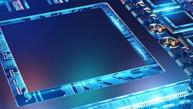
Heterogeneous Integration of Chiplets Using 3D IC
The method of fabricating a device on a single piece of silicon, known as monolithic semiconductor fabrication, is not affordable, expedient or low risk. As processing demands and the need for scalability rise, system-on-chip (SoC) is less likely a future solution. More is now expected than what Moore’s law originally anticipated.
The solution, a homogenous SoC disaggregated into function-specific chiplets. Through heterogeneous integration using 3D IC packaging, chiplets can be mixed, matched, and merged for increased, diverse functionality.
Watch the on-demand webinar to learn how heterogeneous integration improves IC design.
3D IC packaging: heterogeneous integration and hyper-scalability
Heterogeneous integration using 3D IC packaging provides key advantages that outshine a conventional monolithic SoCs. These include:
- Reduced area of processor core
- Higher speed processor memory interface
- Increased performance
- Product configurability and scalability
See how packaging design workflows can benefit from the emerging chiplet ecosystem and enable hyper scalability. If you’re considering developing or using artificial intelligence, learn why you should consider heterogeneous integration to optimize your designs through specific project objectives.
Why consider heterogeneous integration to optimize your 3D IC designs?
If design and package teams set and follow certain codesign tenets, the heterogeneous integration of chiplets is a game-changer for any application that necessitates high-compute components and diverse functionality. Modern, cutting-edge applications such as artificial intelligence, HPC, 5G, IoT, and consumer mobile will benefit from 3D IC designs, driving an electronic device demand that presses the need for ever-increasing performance at ever-decreasing costs.